  |
      |
|
|
|
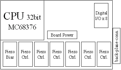
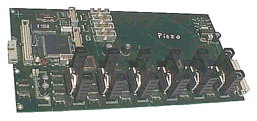
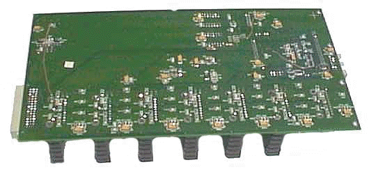
CPU core : This block is the core of the modular design approach. It consists of a MC68376 made by Motorola, which is a 25 MHz micro controller with the following on chip peripherals. One RS232 serial channel for communication to the host computer (PC, running Win98, etc�). Eight 10 bit ADC channels (available to an optional daughter board) for analog control application. Four Clock/Data serial loops. One for the on board Digital I/Os. Three for additional peripheral I/O functions or multiprocessor communications (not being used at this board). This isolates the I/O functions from the CPU-buses and results in a very stable CPU design. Thirteen TPU (Time Processing Unit) channels for piezo control or other precision timing operations. Two TPU channels are used by an additional RS232 communications port for software debug, and supervisory functions. The program is stored in 256 kWord (16 bit wide) Flash-Memory with an additional 512 kByte (8 bit wide) S-Ram. The CAN interface as well as the fast on-chip timers are are available on connectors for off-board processing. Piezo control : This particular configuration supports 6 piezos (max config), as well as an optional common piezo bias Voltage. Each piezo has 3 programmable (8-bit DAC) Voltages (-50 V to +50 V) with programmable pulse timings of 20 us min and a max slew rate of 4 us. Digital I/O : There are 8 input/output lines available per block, with a total of 1 blocks for this particular configuration. Each consists of a NPN open collector output with a 300 mA current capability. The total, at one time, on current has to be less than 4 A. This output is being monitored by the input portion of the digital I/O node. If the output is in the off state, the input can be used as a general purpose input for monitoring switch closures, etc,. All CPU-board based I/O nodes are being processed in sync at a 3 ms period.
|
|
We are sure that You still have some questions or comments, so
please contact us at
|